 In my previous blog post on RS-232 with the Altera Cyclone II FPGA, I demonstrated how to create a serial echo by simply connecting the Tx wire and the Rx wire together. That’s a great start, but the goal is to be able to read the data in the FPGA and do something with it. The single-wire input signal alone doesn’t solve that problem; we need a receiver component that is able to translate that wire to a digital byte stream.
In this post, I’ll demonstrate how to add third-party receiver and transmitter components to translate between the serial wire and the byte stream. For this project, you can start with the end-point of the previous entry.
For the first step in this tutorial, we need to add serial port receiver and transmitter components to our existing canvas. Unfortunately herein lies the problem — Altera Quartus doesn’t ship with a serial port receiver or transmitter component in the symbols library, so we have to add our own!
Fortunately we don’t have to reinvent the wheel.
If you look around on the internet, there are plenty of open-source libraries for creating RS232 encoders/decoders. The one I used is this simple one from fpga4fun. (The link to download the actual code is the bolded HERE at the bottom of that page, or here’s the direct link if you want to download it directly). There are good explanations of this codebase, along with other protocols, on that website, so I won’t go into the details here. We’ll just assume the code is correct and I’ll show you how to use it in your project.
Download and unzip the async.zip file from the website, grab the two Verilog .v files and place them in your project directory. Before we can use these files as components that we can drop on our canvas, we need to generate symbol files.
To do this, open the two files in Quartus (File>Open), and it’ll show each in a code editor tab. Select the async_transmitter.v tab, and click File>Create/Update>Create Symbol Files for Current File. It’ll chug for a bit, and then finally show a dialog saying it was successful. Do the same thing for the async_receiver.v tab. This process creates the symbol files so that we can place the components on our design canvas.
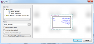
Let’s do that now. Double-click the canvas, and that brings up our symbol list. Now you should be able to see our newly-compiled components in the symbol list!
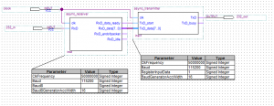
You can see just from the diagram roughly how these components work. The RxD is the input to this component, straight from the RS232 input wire. The receiver waits for data coming down that wire, and when it gets what it decodes as a byte, it sets the RxD_data output bus and triggers the RxD_data_ready signal so you can do what you want with it. In our case, we’ll just feed that data straight to the transmitter, and trigger its “start” action.
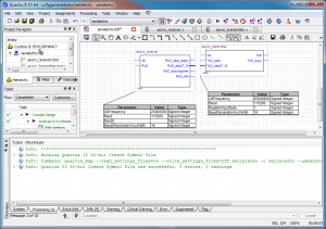
Click OK, and place each one of these parts. Your canvas should look roughly like this now:
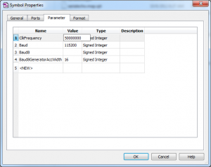
Now, one quick change we have to make—the clock frequency of the starter board is 50 MHz, not 25. So double-click each of the parameter lists, and make that change.
Great! Now we’ve got our big components laid out, so now all we have to do is add I/O pins for the serial port, an input pin for our clock, and hook everything up. Let’s do that now.
To add the pins, you could double-click the canvas and search for the I/O pins among the symbols, and add them the same way we did our ports, but there’s a shortcut. The icon right above the canvas that looks like this is a pin placement shortcut. Use this to place two input pins and one output pin on the canvas. Double-click the names of these to rename them to “clock”, “232_in”, and “232_out” respectively.
Now we have to wire everything up. We want the clock to feed both components, the 232_in to feed the receiver’s RxD, the receiver’s RxD_data and data_ready to feed the transmitter’s TxD_data and start, respectively, and the transmitter’s TxD to feed the 232_out. The final diagram should look like this:
Now the final design step is to assign the pins in our diagram to actual pins on the chip. To prepare for this, choose Processing > Start > Start Analysis & Elaboration. This will churn for a while and lets Quartus pre-populate your pin settings with the names of the pins you’ve given above.
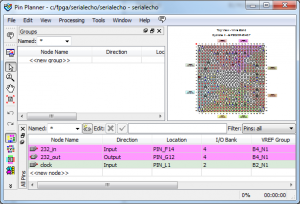
Now select Assignments > Pin Planner. For this step, we have to look up in the design spec which pin ID’s correspond to the serial and clock pins. We find that the clock is L1, the 232 input is F14, and the output is G12. We add those locations to the editor, and it should end up looking like this:
You’ll also note that on your canvas, it adds a note to each pin symbol.
And that’s it! We can now compile the project and load it onto your board. Follow the steps in my previous blog post to compile, load, and test the app, and you’ll see the serial port echoing your bytes back at you.
Except wait — it’s only echoing back every other byte! Yup, there’s a bug. Apparently the transmitter takes an extra clock tick to transmit the byte, so when the subsequent byte is ready from the receiver, the transmitter isn’t ready yet and it drops. However, the important thing is we’re now decoding and encoding actual bytes, and clocking that data in on a reusable clock signal, so we are now able to process that data however we want. We’ll explore using this ability to add other features in future blog posts.
This blog post is Part 2 in a series. To review Part 1, you’ll want to Go Here. To view Part 3, you’ll want to Go Here.
One Response
So 8 years later in 2021 I was able to get this work with the current files at http://www.fpga4fun.com with a tiny change. The downloadable file at fpga4fun contains one file async.v which I then split into three files: async_transmitter.v, async_receiver.v and baudtickgen.v.
I opened all three in my Quartus Prime Lite 20.1.1 project and created symbols for async_transmitter.v and async_receiver.v
This worked fine and was tested on my EP4CE10 based board. However the “bug” of every other character is _not_ present.
Thought this might be useful for someone trying to get started with RS232. Note that in my case my board has USB (CH340G) and that worked just fine with this tutorial. (I used PuTTY on W10.)