 In my first blog post on communicating with the Altera Cyclone II FPGA, I demonstrated how to create a serial echo by simply connecting the Tx wire and the Rx wire together. Then in my second post I demonstrated how to use third-party libraries and a clock to allow that serial line to be translated into a byte stream and back before being re-transmitted to the host. In this post I’ll show how to write custom Verilog to process the data that is received.
As a software developer, this is the part of FPGAs that interests me the most. If you’re reading this post, I’m sure you’re aware of the fact that an FPGA can provide massively parallel computation in a way that a CPU or even a GPU is unable to achieve. The difficulty is in getting started. You can’t just download a C library and link to it like you can with CUDA. You instead have to roll up some means of communication and write code to send the raw and processed data back and forth. For most high-level software designers like myself this is far from straightforward. Hence, this series.
So, on to the good stuff. We left off last time with third-party components for a transmitter and a receiver that were hooked up directly to each other. For this lesson we’re going to create a new Verilog component that takes the first ten bytes of the serial stream, reverses them, and then sends them back to the PC. The following assumes that you have gone though the previous posts and have finished the Quartus project of Part 2.
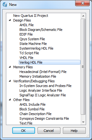
The first step is to create the new Verilog file and add it to the project. So click File > New, and select Verilog HDL File.
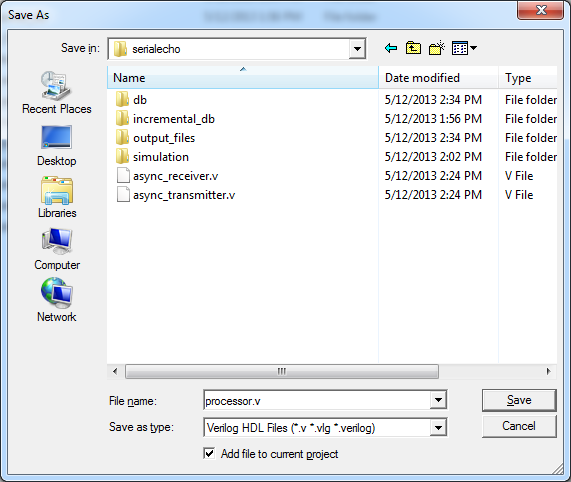
Go ahead and save the file as “processor.v”.
At this point we start coding. This blog post isn’t intended to be an introduction to Verilog, so I’m not going to go into great detail over each line of code here. But, the general idea is, we’ve got a state machine with a READ state, a SOLVING state, and two WRITE states. The READ state reads data until the 10th byte is received, then switches to SOLVING. The SOLVING state reverses the array (all in one clock tick!) and switches to WRITE1. Finally the WRITE states wait for the txBusy signal to go away, transmit the next byte, and repeat. (There’s probably a way to combine WRITE1 and WRITE2 into one state but this is the first thing I got working).
Here is the full source of processor.v
|
1 2 3 4 5 6 7 8 9 10 11 12 13 14 15 16 17 18 19 20 21 22 23 24 25 26 27 28 29 30 31 32 33 34 35 36 37 38 39 40 41 42 43 44 45 46 47 48 49 50 51 52 53 54 55 56 57 58 59 60 61 62 63 64 65 66 67 |
module processor(clk, rxReady, rxData, txBusy, txStart, txData); input clk; input[7:0] rxData; input rxReady; input txBusy; output reg txStart; output reg[7:0] txData; localparam READ=0, SOLVING=1, WRITE1=2, WRITE2=3; localparam LEN = 10; localparam LENMAX = LEN - 1; integer ioCount; reg[7:0] data[0:LENMAX]; integer state; initial begin txStart = 0; state = READ; end always @(posedge clk) begin case (state) READ: begin if (rxReady) begin data[ioCount] = rxData; if (ioCount == LENMAX) begin ioCount = 0; state = SOLVING; end else begin ioCount = ioCount + 1; end end end SOLVING: begin integer i; for (i = 0; i < LEN/2; i = i + 1) begin reg[7:0] swap; swap = data[i]; data[i] = data[LENMAX-i]; data[LENMAX-i] = swap; end state = WRITE1; end WRITE1: begin if (!txBusy) begin txData = data[ioCount]; txStart = 1; state = WRITE2; end end WRITE2: begin txStart = 0; if (ioCount != LENMAX) begin ioCount = ioCount + 1; state = WRITE1; end else begin ioCount = 0; state = READ; end end endcase end endmodule |
This is different from traditional code in that all this stuff is happening in parallel. For example in READ, there’s no loop to read 10 bytes. Instead, this entire block gets executed each clock tick, so you update your data array, increment your counter, and update your state to SOLVING if it’s read 10 bytes.
The exciting part is that the SOLVING block also happens as one clock tick. Here we’re doing nothing much, just reversing a small array. However you can imagine the potential, to do enormous computations here and it would just take a few clock ticks. For instance I have a sudoku solver that typically requires only 6-7 ticks to solve a full puzzle (perhaps a topic for a future post).
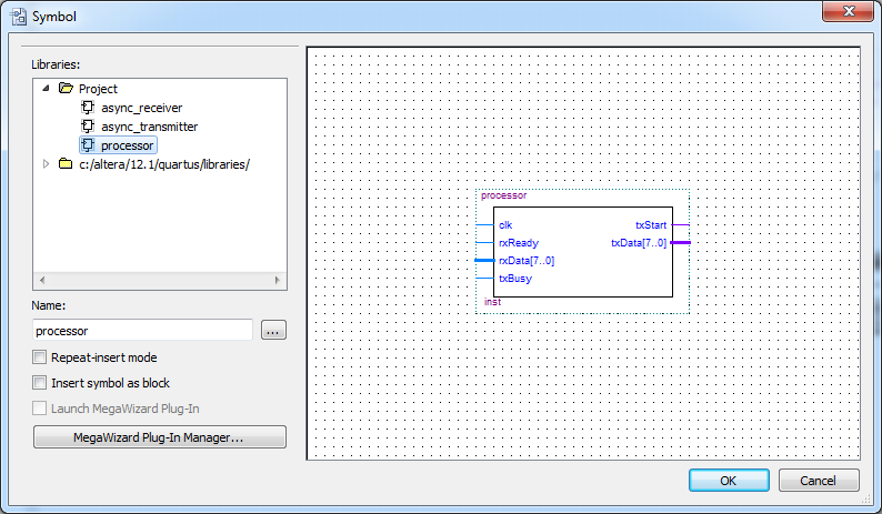
Anyway, now that we’ve got the code we have to insert it into the board design. So, as in Part 2, the first thing you have to do is create a “symbol file”, so click File > Create/Update > Create Symbol Files for Current File. Now we can add it to the board design, so double-click on the board, and you’ll see your shiny new “processor” symbol. Select OK and add it.
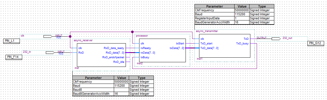
You’ll now want to hook up the processor to the receiver and transmitter. The links should be self-describing, but if you need help the final design should look like this:
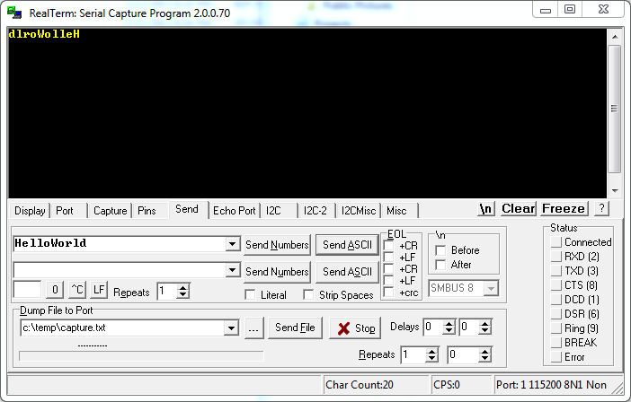
Now we compile and load the code on the FPGA just like last time, and that’s it! Open your favorite terminal, and take it for a spin!
As I mentioned earlier, this FPGA example was pretty trivial, but this series has demonstrated an easy way for a beginner to get up to speed using an FPGA for data processing and communicating with it over the serial interface, which is a big hump for software engineers with little low-level hardware exposure. From here, it should be straightforward for any good developers to experiment with new algorithms or ideas that they have in mind.
This blog post is Part 3 in a series. To review Part 1, you’ll want to Go Here. To review Part 2, you’ll want to Go Here.
3 Responses
amazing job, however, can you provide the same codes in part 2,3 in vhdl, that would be amazing , thank you
hello sir, any tutorial altera de1 sending serial data to serial terminal. Example press button key0 then in serial terminal will show KEY0 Pressed.
To be able to create the symbol for processor.v I needed to change line 38 of the code to “for (i = 0; i < LEN/2; i = i + 1) begin"
I am guessing this is due to a tiny difference in syntax with Quartus Prime Lite version 20.1.1 after 8 years. (In 2021.)
I thought this might be a useful note for someone trying to follow along with the tutorial in 2021. It worked with USB (CH340G) on my EP4CE10 based board. (I used PuTTY on W10.)