 Other than years of experience, a polished resume, and the ability to design circuits on a white board with 3 hiring managers looking over your shoulder, what can an electrical engineer do to stack the deck in their favor when looking for a job? In our previous blogs, we’ve outlined the importance of a PE license. Being a professional engineer is the number one thing an electrical engineer can do to stand out, especially because it’s something most electrical engineers do not pursue. One of the next best things an electrical engineer can do is to become an IPC Certified Interconnect Designer (CID).
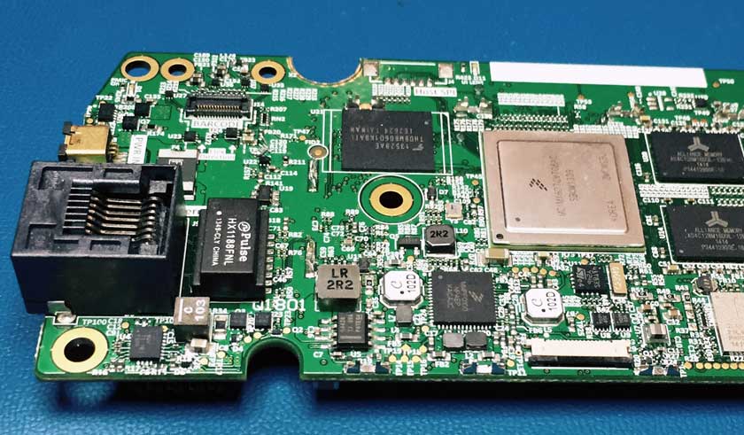
If you’ve designed a PCB, you probably find yourself wondering about the finer details of PCB design that you may be missing. Your design works, but are you sure it’ll have the reliability and performance that you need? Early in my career, I could design a schematic, use various pcb layout tool, and build a working board, but I knew there were many aspects of the design that I did not fully understand.
How do I select my board stackup, and what’s a pre-preg? What can I leave up to the manufacturer, and what choices are important that I make myself? How do I size annular rings, through-holes, and surface mount pads for optimum reliability? How do I size thermal relief to a pad? How do I appropriately select trace thickness for higher currents? What about spacing for high voltage?
The answer to all these questions can be found in IPC-2221 (Generic PCB design) and IPC-2222 (Rigid PCBs). IPC teaches a Certified Interconnect Designer (CID) and a more advanced CID+ course that teach a designer how to design circuit boards according to these two standards. Multiple engineers at Sparx have our CID, and we all walked away from the course with a better understanding of how to design the best, most robust PCBs possible.
Example: High Voltage, High Current Design
I can’t go through examples of all the benefits of understanding these standards but here’s an example of how they can be very useful. I was recently working on a system powered from a 150 Volt Lithium Ion battery pack. The board that I was designing was small in size and had many high speed signals mixed in with 150V DC that powered a motor control that could draw 20-30 amp peak. There’s a lot that could go wrong with this layout. Safety, thermal properties, impedance control, and arc prevention were just a few things that have to be considered.
 High Current: IPC-2152 has graphs and formulas to calculate trace/plane width. The Saturn PCB Toolkit calculates this nicely based on the IPC Standard. This tool can help determine if you need a heavier weight copper. If you have 25 Amps running through a PCB trace or plane, but can’t use a big plane, then the typical 1 oz copper won’t cut it.
High Voltage: IPC-2221, Table 6-1 spells out the minimum spacing for internal and external layers for various situations (sea level or elevated, coated or uncoated). 25 mil is the minimum copper to copper spacing at 101-150 V, uncoated, at sea level to 3050 meters. Keep spacing greater than that when possible, and, of course, keep signals away from 150 V.
Thermal relief: Say you have a through hole pin with high current, and you’re using 4 oz copper to handle all of that current. You better not direct-connect to your power plane or it’s going to be really tough to solder and even tougher to ever replace. Also, if you multiple ground layers, be careful about not connecting too much copper to a through-hole pin thats tied to the ground net. IPC-2222, 9.1.2 goes into lengthy detail on how to size thermal reliefs.
There are many more examples of how these standards have aided me in design. Tools like the Saturn Toolkit are very nice for a quick reference, but without knowing the IPC standards, you may be missing out on a lot of good design guidelines.
3 Responses
The IPC Certification process ensures that applicants acquire: Understanding and knowledge of IPC technical standards, protocols, and guidelines; Skills to apply the IPC approach and engage in IPC Analysis; Capacity and experience to lead IPC Training and Analysis. Our each Master IPC Trainer has over 13+ years of experience in assembly, inspection and training in the electronics manufacturing environment.
Hello, @Dchesney!!!
Being an IPC Certified designer, can also help in getting a better job in electronics Industry. And yes, @Soldertraining also said correctly that IPC Certification process ensures that applicants acquire: Understanding and knowledge of IPC technical standards, protocols, and guidelines along with various skills to apply the IPC approach etc. Nowadays, with the advancement in technology, thing are also becoming more complex which makes compulsory to go through some specified courses. So, thanks for this wonderful blog post and sharing such an informative content with us.
Totally agree with you, Katy,
IPC Certification really plays an important role in getting jobs in the electronics industry. Thanks for sharing such useful information @dchesney.