I’ve been interested in learning how to program FPGAs, and I recently purchased a Cyclone II FPGA Starter Board from Altera to learn some of those skills.
It comes with a few tutorials on how to make the LEDs blink and such, but nothing more than that. That’s great, but if you’re wanting to do any kind of numeric processing, there’s no way that blinking LEDs can give you the feedback you need to determine if your algorithms are right. You need some way to be able to communicate over a serial port. I’ll present a series of posts on how to get you up and running with a new dev kit. In this first one, we’ll simply create a project that echoes your serial port back to you. In that process, we’ll learn how to create projects, place and map pins, and program the FPGA.
You may want to follow along with Altera’s LED blinker tutorial in parallel, in case I left some steps out.
First thing, get rid of the outdated Quartus CDs that came in the box, and download and install the most recent version of Quartus II Web Edition directly from Altera. This is a huge download, so use a fast connection!
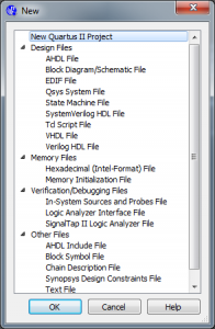
This takes a while to install too, but go ahead and accept the defaults and grab a cup of coffee. Once it’s finished installing, you’re ready to roll with FPGAs. Click the icon to launch Quartus II Web Edition, select File > New, and create a new project.
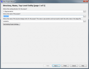
On the first page of the wizard, set up your working directory and project name. Note that you probably don’t want to take the defaults here, as they put everything into your install directory, and also note it doesn’t automatically create a subdirectory with the name of your project, so you have to specify that yourself. Go ahead and use “C:fpgaserialecho” as the directory, and “serialecho” as the name.
Page 2, just click Next.
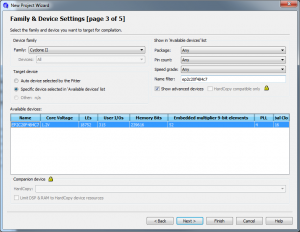
On page 3, choose the Cyclone II family, and the device name is “EP2C20F484C7”, as you can see by looking at the chip. (Ignore the “n” at the end of the name—that just means it’s a lead free chip, as you can see in section 6-2 of the Cyclone II Handbook).
On page 4 and 5, just click Next and Finish to create your new project.
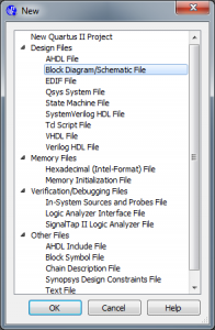
Now, we need a top-level schematic to lay out our components. So click File>New, and choose Block Diagram/Schematic File.
That’ll create your design canvas, which you should see on your screen. So now save it (you have to click “Save As”), and feel free to take the default name, which should be the same as your project.
Great! Now all we have to do is add I/O pins for the serial port, and hook everything up. Let’s do that now.
To add the pins, you could double-click the canvas and search for the I/O pins among the symbols, but there’s a shortcut. The icon right above the canvas that looks like this is a pin placement shortcut. Use this to place one input pin and one output pin on the canvas. Double-click the names of these to rename them to “232_in”, and “232_out” respectively.
Now we have to hook them up. Since echo is simply looping the Rx back onto the Tx line, all we have to do is connect the two symbols with a wire. The final diagram should look like this.
Now the final design step is to assign the pins in our diagram to actual pins on the chip. To prepare for this, choose Processing > Start > Start Analysis & Elaboration. This will churn for a while and lets Quartus pre-populate your pin settings with the names of the pins you’ve given above.
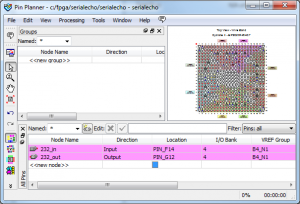
Now select Assignments > Pin Planner. For this step, we have to look up in the design spec which FPGA pin ID’s correspond to the serial pins. We find that the the 232 input is F14, and the output is G12. We add those locations to the editor, and it should end up looking like this:
You’ll also note that on your canvas, it adds a note to each pin symbol.
And that’s it! We can now compile the project and load it onto your FPGA board. Press the play icon to compile it. To the right there’s a diamond-shaped icon that gives the tooltip “Programmer”—click that one to bring up the programming dialog. With your FPGA dev board plugged into the USB port and turned on, click the Hardware Setup button, select the USB-Blaster option from that dropdown box and press Close.
Now you should be able to use your favorite terminal tool at 115200 baud and see data being echoed back to you over a serial port. I only had to use a gender changer to hook it up to a standard serial cable, but when using a USB-serial adapter, I also had to add a null-modem adapter. If one doesn’t work, then try the other. If neither work, then make sure you’ve got your pins assigned correctly; I initially had the assignments reversed and it took me a good fifteen minutes before I figured out what was wrong.
Next time we’ll look at adding some custom components for encoding and decoding between these serial streams into actual bytes on the FPGA.
This blog post is Part 1 in a series. To view Part 2, you’ll want to Go Here. To view Part 3, you’ll want to Go Here.
